Powering North America's Future, One Chip at a Time
Great Lakes Semiconductor (GLS) is incorporated in Ontario, Canada, with its headquarters located in Markham, Ontario, Canada. Once fully established, GLS will be a full-scale semiconductor company focusing on developing world-class semiconductor fabrication facilities and technology park ecosystem aimed at addressing critical needs in Canada’s semiconductor industry.
GLS initially will include: research, design and development of chips, chip sets, and other mems/sensor devices; workforce development; establish a pocket fab for prototype and small-lot production; and build a new, state-of-the-art full-scale chip manufacture at 200mm and 300mm process technologies. In collaboration with its strategic partners, such as Canada’s ventureLab, GLS will focus on expanding and securing Canada’s semiconductor supply chain.
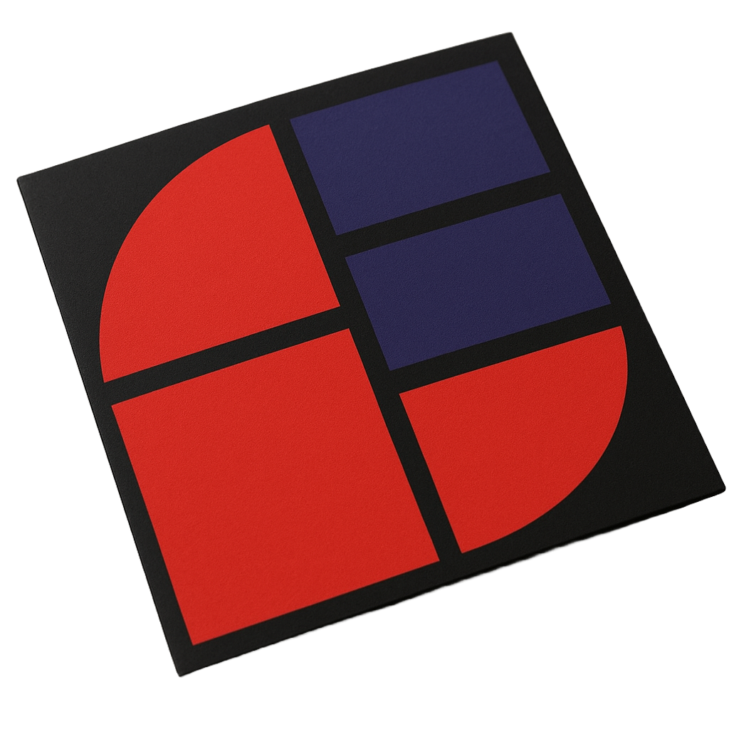
Our Logo
Our logo has true meaning. Consisting of five pieces they represent so much more than a traditional logo. We all have 5 major senses, which is symbolic of the sensors GLS will be primarily manufacturing in our early years of operation. Also in Japanese culture, there are 5 elements: Earth, Wind, Fire, Water and the Void. In Chinese and Korean cultures, the 5 elements are: Earth, Fire, Water, Metal and Wood.
Our logo was designed keeping all of this in mind, along with other symbolizations….
Hub and Spokes of Great Lakes Semiconductor in Ontario
- The Hub and Satellite Hub = the Fab/Technology Park in Pickering (Durham Region) represented by the large red square block in the lower left-hand quarter; and the curved red block in the lower right-hand corner as the Pocket Fab and ventureLabs in Markham.
- The Spokes = Durham, York, Pelle, Halton, Waterloo, Niagara
Red, White (Lines) & Blue for the US and Red for Canada. The white lines also symbolize a chip’s circuitry.
Canada’s Maple Leaf
Five core elements of the semiconductor manufacturing process:
- Wafer Fabrication (front end. Processing)
- Lithography (patterning)
- Deposition & Etching (thin film processing)
- Interconnect and metallization
- Packaging and Testing (back-end processing)
The 5 bodies of water that border Ontario:
The Great Lakes of – Erie, Ontario, Superior, and Huron, and the St. Lawrence Seaway.
The 8 US States bordering the Great Lakes:
Illinois, Indiana, Michigan, Minnesota, New York, Ohio, Pennsylvania, and Wisconsin
The 5 major Canadian Indian Nations:
- Haudenosaunee Confederacy (Iroquois/Mohawk Confederacy).
- Anishinaabe
- Cree Nation.
- Dene Nation.
- Coast Salish Nations.
The 5 core business principles of Great Lakes Semiconductor:
- Innovation & integration – the smooth, rounded edges represent seamless integration of our semiconductor technologies with Canada’s high-tech industry.
- Collaboration & connectivity – reflecting the interconnected nature of semiconductor manufacturing and the broader supply-chain ecosystem especially in the technology park.
- Fluidity & Precision – inspired by the Great Lakes, the rounded edges could symbolize water, fluidity, and precision engineering in chip fabrication.
- Balance of tradition & future – the logo is a modern version of the maple leaf as an element of Canada’s identity, while the rounded edges modernize and soften it for a forward- looking vision.
- Scalability & growth – the curves also suggest adaptability and growth., essential for a Class 1000 Pocket Fab as well as a major Class 1 cleanroom evolving from prototype to production.